|
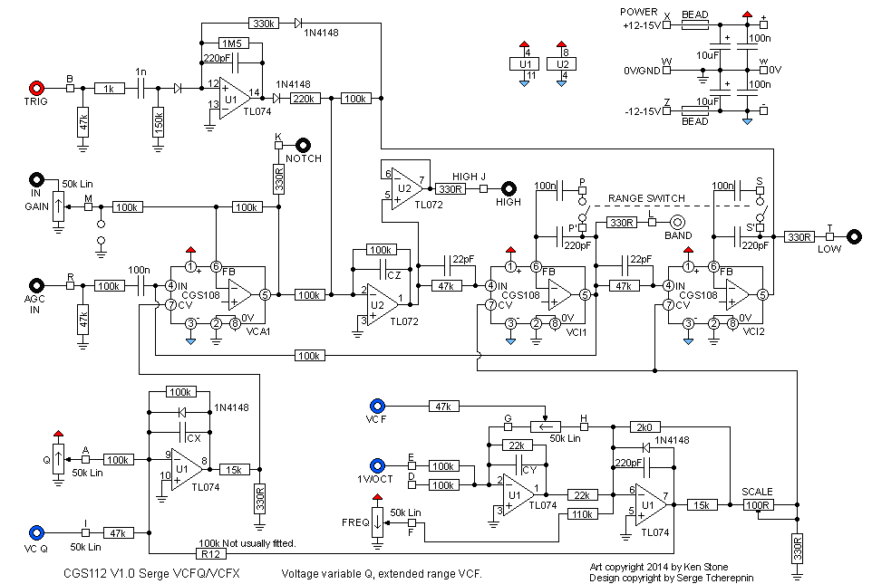
This module is a variation on the Serge Voltage Variable Q VCF module (VCFQ) and the Extended Range VCF (VCFX).
From the 1982 Serge catalog:The VARIABLE Q VCF (VCFQ) is an excellent general-purpose VCF offering simultaneous low-pass, high-pass, band-pass and notch (band-reject) outputs. The resonance (Q) of this filter is dynamically variable by manual or voltage control. The VCFQ has two signal inputs. One incorporates an automatic gain control to prevent the filter from overloading at high Q settings. The second input has a level control so that the percussive effects of overloading the filter can be exploited. When a pulse is applied to the Trigger input, the filter will ring, producing a damped waveform similar to that produced by striking a resonant object. The nature of this ringing is controlled by the Q and the filter frequency. Percussive effects ranging from clicks to the sound of wood blocks and bell tones can be produced and controlled. This ringing effect can be used in conjunction with signals applied to either of the audio inputs to achieve highly controlled complex tonal qualities.In addition to the three VCF's, Serge Modular offers an EXTENDED RANGE VCF (VCFX) which is identical to the VCFQ except it features a second sub-audio range. This low-frequency range allows use as a control voltage processor. A fast envelope or trigger applied to the filter in the low range at high Q settings will cause low-frequency ringing, generating complex envelopes and damped vibrato effects. The VCFX can be patch programmed to oscillate by patching the band-pass output to the manual input. The outputs will be in quadrature relationships (90 degrees out of phase). A little on how it works:
Construction
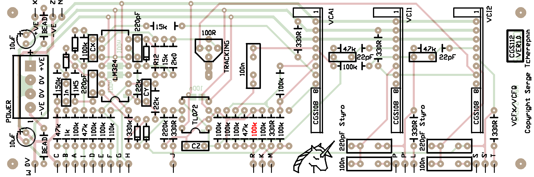
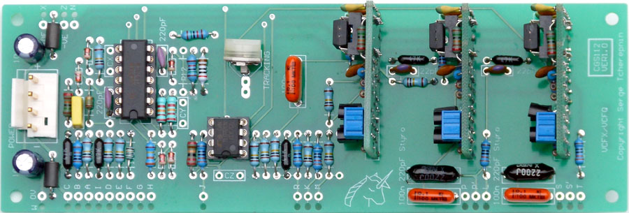
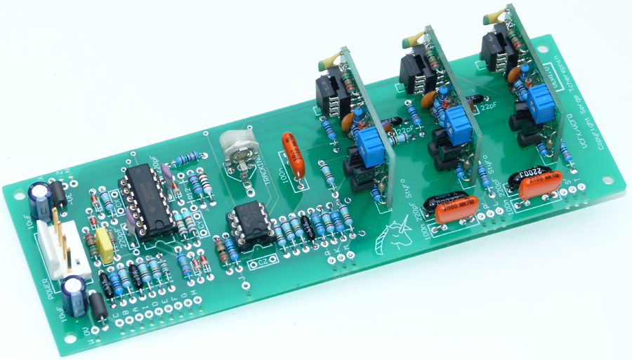
The CGS112 VCFQ uses three CGS108 Serge Gain Cells as it's voltage controlled elements. Refer to the CGS108 page for construction details. The boards are built exactly as per that page. They should be the last things you install on the CGS112 PCB. Before you start assembly, check the board for etching faults. Look for any shorts between tracks, or open circuits due to over etching. Take this opportunity to sand the edges of the board if needed, removing any splinters or rough edges. When you are happy with the printed circuit board, construction can proceed as normal, starting with low profile components such as resistors and diodes first, followed by successively taller components. Take particular care with the orientation of the polarized components, such as ICs, electrolytics, diodes, and transistors. When inserting the ICs in their sockets, if used, take care not to accidentally bend any of the pins under the chip. Also, make sure the notch on the chip is aligned with the notch marked on the PCB overlay.
R12: This resistor is not usually fitted. If a 100k is soldered in this position, the frequency controls will also affect the Q.
The 1M resistor connected to pad R is incorrectly marked. It should be 100k. The unit will run on either +/-12 volts or +/-15 volts. Serge suggests that linear pots of 50k are suitable for use. My prototype uses 100k pots without trouble. The first time you power it up, I would suggest you do so with 22 ohm resistors in series with the positive and negative power rails. This should save the chips if you have made a blunder.
Set UpThe only trim pot on the CGS112 PCB is adjusted to give a 1 volt per octave response. See the VCO page for suggestions on how to set this. It is probably easier to adjust while the filter is set to self oscillation (Patch IN 2 to BP output, and turn up GAIN pot). From Serge kit instructions:
Test Procedure; Notes:
Parts list This is a guide only. Parts needed will vary with individual constructor's needs. If anyone is interested in buying these boards, please check the PCBs for Sale page to see if I have any in stock. Can't find the parts? See the parts FAQ to see if I've already answered the question. Also see the CGS Synth discussion group.
Article, art & design copyright 2013 by Ken Stone
| ||||||||||||||||||||||||||||||||||||||||||||||||||||||||||||||||||||||||||||||||||||||||||||||||||||||||||||||||||||||||||||||||