|
This module is a variation on the 1973 Classic Serge Triple Wave Shaper module. To quote the 1982 catalog: The Triple Wave Shaper (TWS) is a non-linear modifier which can transform a sawtooth wave into a sine wave. This module incorporates three independent wave shapers for modifying synthesizer waveforms or for processing signals from preamplified instruments. Although originally designed as a wave shaper for our early oscillators, this module has been found to be a excellent modifier of electronic and acoustic sounds, and is highly recommended for subtle timbrel modifications beyond the range of simple oscillator/filter patches. Of course, it's uses go beyond this. When used in series, they can be used to add folds to the wave shape. Each extra wave shaper you put in series adds a fold to the waveform. As such, quite a lot of tonal variety/harmonic enrichment can be achieve.
A little on how it works:
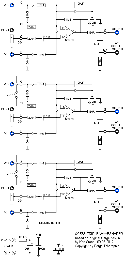
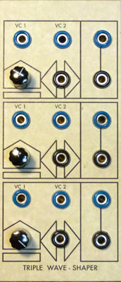
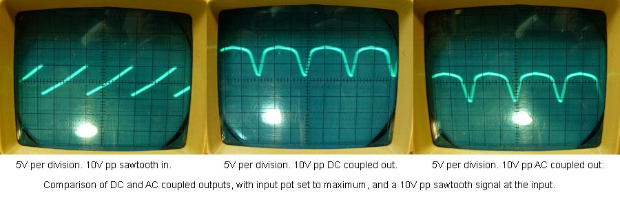
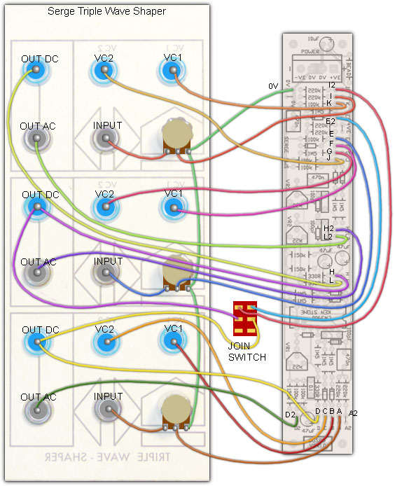
On the 1973 version of the Tripe Wave Shaper, all of the input pull down resistors were 22k, not 100k as shown in this schematic, and the components for the AC coupled outputs were mounted on the back of the jacks themselves. By around 1975, these AC coupled outputs were dropped, and both output jacks were simply linked. The output is usually in the 0-5V region. The AC coupled output "centers" it around 0V, an apparent offset varying with wave shape. 25k pots were used for the input level controls. Later two-column panel designs dropped the second outputs altogether, and added a Join switch that coupled the three shapers together. The pots were moved from the PCBs to the panel, but the PCB remained essentially unchanged. On the schematic for the CGS85 version shown here, additional 220k input resistors have been added, allowing for a Join switch while preserving the individual inputs, unlike the original, which disconnects them. The new Join switch wiring connects all three wave shapers in series, but allows input and output connections to each shaper. If using this Join switch wiring option, the input pots for the second and third shapers are bypassed, and have no effect on the signal coming from the previous shaper. They do, however, allow mixing in an additional signal connected to the corresponding shaper input. If you still wish to use the "classic" joining of the modules, it can easily be arranged by leaving the Join switch off, and using patch cords between the three shapers. 100k pots have been used, bringing the input impedance up to the modern standard of 100k.
Construction
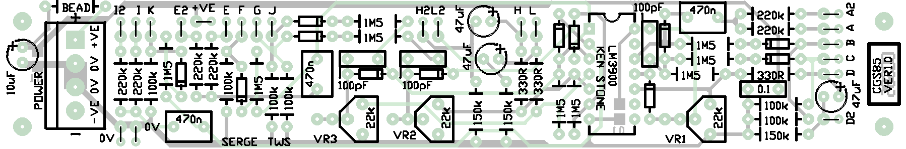
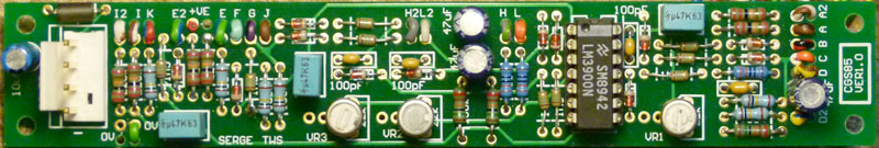
Before you start assembly, check the board for etching faults. Look for any shorts between tracks, or open circuits due to over etching. Take this opportunity to sand the edges of the board if needed, removing any splinters or rough edges. When you are happy with the printed circuit board, construction can proceed as normal, starting with the resistors and diodes first, followed by the taller components. Take particular care with the orientation of the polarized components, such as electrolytics, diodes, ICs and transistors. Traditionally, when the join switch is used, the signal is fed into the bottom wave shaper, and taken from the top one. As such, the top stage on the schematic is the bottom stage on the panel.
Set UpIf you have fitted a "join" switch, switch it off. If you have access to a CRO, use it. If not, a multimeter set to the AC volts position can be used. Plug an audio frequency sawtooth wave into the IN jack on the top section. Monitor the OUT jack while turning the knob to fully clockwise. Adjust the appropriate trim pot until the output level is approximately that of the input. If using a meter, read the voltage on the input. It doesn't matter what the actual value is, as it probably won't be accurate. Adjust the trimmer until you get approximately the same voltage on the output. Repeat for each stage. Control voltages applied to VC1 and VC2 should then modify the shape of the output wave.
For those interested, original Serge kit assembly and set-up instructions can be found here:
Notes:
Parts list This is a guide only. Parts needed will vary with individual constructor's needs. If anyone is interested in buying these boards, please check the PCBs for Sale page to see if I have any in stock. Can't find the parts? See the parts FAQ to see if I've already answered the question. Also see the CGS Synth discussion group.
Article, art & design copyright 2011 by Ken Stone
| ||||||||||||||||||||||||||||||||||||||||||||||||||||||