|
Dev-mod Mixer/Inverter block for music synthesizers.
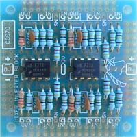
While this "development module" does replicate the D.C. Mixer to some extent, the intended use is a little different. When prototyping new designs, on frequently fines the need to build certain component blocks over and over again. The options are simple - waste time doing it again, waste a good board to use the subsections that are required, or use something like this, that can be easily salvaged after each use. If course there is nothing to prevent it becoming a permanent part of a one-off design either. A little on how it works:
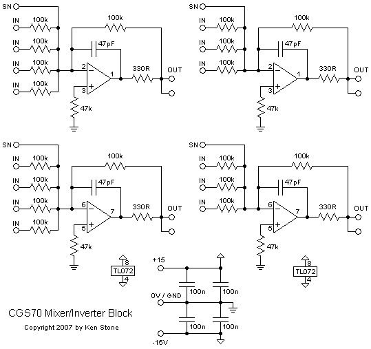
The schematic for the Mixer/Inverter Block.
Each of the blocks is functionally identically and can be configured in several ways. Each block is quite conventional, using a single op-amp in a unity gain inverting configuration. Each block allows three or four DC signals to be summed, as well as providing a summing node (SN) to which more resistors can be connected if desired. The result of the summing is inverted around 0V, making it passable for use with summing audio signals, but less satisfactory for control voltages, unless inversion is what you wish to achieve. To deal with this, the output of a block can be connected to the input of a second one to re-invert the signal, coincidentally adding some "inverted inputs" to the mixer should they be required. Each block is designed so its output is load-independant. The circuit board allows the easy connection of one block to the next by providing input and output pads right next to each other, though this does put the signal across two op-amps. For improved isolation between sections, it would be better to use the second block from the same chip to do any re-inverting.
Construction
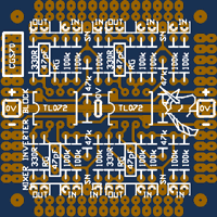
Before you start assembly, check the board for etching faults. Look for any shorts between tracks, or open circuits due to over etching. Take this opportunity to sand the edges of the board if needed, removing any splinters or rough edges. (With the boards supplied by me, the edges are already milled, and etching faults are very rare.) When you are happy with the printed circuit board, construction can proceed as normal, starting with the resistors first, followed by the IC socket if used, then moving onto the taller components. Take particular care with the orientation of the polarized components such as electrolytics, diodes, transistors and ICs. Decoupling capacitors are mounted directly one the rear of the PCB under the chips. You can use 1206 surface mount devices, or with a little lead bending, monoblock ceramics. The over gain of each block can be changed by varying the value of the resistors marked RG (Resistor-Gain). On the schematic these are shown as 100k, which is appropriate for a gain of one. Around the edge of the board are rows of pads suitable for adding headers to allow dev-blocks to be linked together using the CGS72 joiner or plain old pin header jumpers. Apart from the power rails, these are not assigned, so as to allow maximum versatility. You will need to link these pads to the inputs and outputs of the circuit blocks as required. Use 1% metal film resistors for the 100k resistors, both for accuracy and lower noise. Notes:
Parts list This is a guide only. Parts needed will vary with individual constructor's needs. If anyone is interested in buying these boards, please check the PCBs for Sale page to see if I have any in stock.
Can't find the parts? See the parts FAQ to see if I've already answered the question. Also see the CGS Synth discussion group.
Article, art & design copyright 2007 by Ken Stone
| |||||||||||||||||||||||||||||||