Voltage Controlled Divider for music synthesizers. This is an upgraded version of my older voltage controlled divider. It has additional mixing and a comparator at the clock input, additional range, and will now work on 12V if needed, as the internal regulator has been eliminated. Details of the earlier versions can be found here. This was originally developed a timing accessory for a sequencer I was working on, though when fed from a VCO, interesting frequency trills like those of the old 8-bit computer games can be produced. Feeding the control voltage from a Psycho LFO produces some interesting effects. There are two outputs, one a narrow "trigger" pulse, the other following the pulse width of the incoming signal. This means that any mark/space ratio sweep being applied to a VCO connected to this module, will also be on the output signal of this module. The division can be varied from divide by 1 to approximately divide by 60. How to use this module: Connect the input to a signal source such as a VCO, LFO or sequencer master clock. Use the control voltage input to determine the number of incoming pulses per output pulse. There are two pulse outputs, marked HO and LO on the PCB. HO (High Frequency out) gives a narrow trigger pulse output. LO (Low Frequency out) gives a pulse output, the width of which varies with the pulse width of the incoming signal. Depending on the individual ICs you use, the propagation delays of the chips will limit the speed at which the LO output can function. I estimate it drops out above 10 kHz, though as mentioned, it does vary with individual 40106 chips. Experiment with it. A little on how it works:
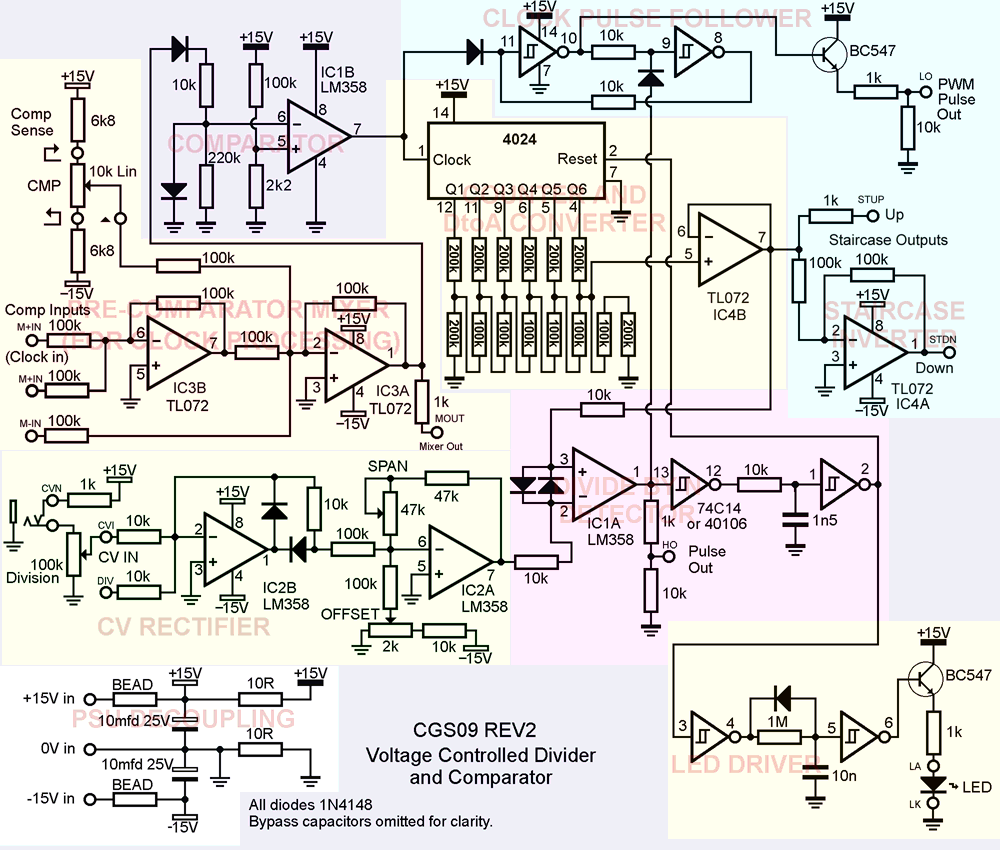
The schematic of the Voltage Controlled Divider. The Voltage Controlled Divider consists of several distinct blocks, each which is fairly simple in its operation. The circuitry around IC1B processes the incoming frequency, and squares up the waveform so it is suitable for the digital portions of the circuit. It drives the counter (4024) and sets the output flip-flop based around two portions of the 40106. This block is fed via a DC mixer stage which includes both inverting and non-inverting inputs, as well as a DC offset allowing for easy adjustment of the "sweet spot" for the incoming signal. The mixer also has an output making the unit a handy utility module even when you are not doing any dividing. The output of the counter (4024) is connected to a D to A converter made using an R/2R resistor ladder. The incoming pulse train will step the counter (4024) until the voltage on the output of the D to A converter is greater than that on pin 2 of IC1A, at which point the output of IC1A changes state, putting a HIGH on the HO output, resetting the flip-flop, and triggering a short delay that resets the counter to zero. This clears the HO output back to LOW. The flip-flop drives the LO output through a transistor buffer. IC2 is dedicated to processing the incoming control voltage. The first part of the circuit is a precession half-wave rectifier, blocking any CV that goes below 0 volts. The second part is used to set the minimum and maximum of the voltage presented to IC1A, as going past either end of the operating range results in either silence or an unpredictable oscillation. (Divide by 0 is NOT very practical!)
Construction
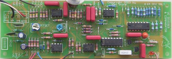
The component overlay. There are two unmarked capacitors near the power connector. These can be ignored, or if you prefer, have decoupling capacitors installed in them. Any 100n capacitors would do. Before you start assembly, check the board for etching faults. Look for any shorts between tracks, or open circuits due to over etching. Take this opportunity to sand the edges of the board if needed, removing any splinters or rough edges. When you are happy with the printed circuit board, construction can proceed as normal, starting with the resistors first, followed by the IC socket if used, then moving onto the taller components. Take particular care with the orientation of the polarized components such as electrolytics, diodes, transistors and ICs. When inserting ICs into sockets, take care not to accidentally bend any of the pins under the chip. Also, make sure the notch on the chip is aligned with the notch marked on the PCB overlay.
SetupThis module requires setting up. Feed an audio signal into the Clock In input. Monitor the output at HO Pulse Out. With the control voltage set at 0 volts, adjust the OFFSET trimmer until the input frequency equals the output frequency. With the control voltage set at the maximum (15 volts if wired as per the diagram), adjust the SPAN trimmer until you get the lowest frequency possible. If the output stops then back up until you get a signal again. Important. The first run of PCBs has a minor error - the voltage follower IC4B (center bottom of the PCB) has its wiring confused. The track between pin 5 and 6 must be cut, as must be the incoming trace that connects to pin 6. This trace is then wired to pin 5, and pin 6 is wired to pin 7. Refer to the PCB/overlay diagram above when correcting the board. PCB connections:
HO High frequency usage output (fixed pulse).
Notes:
Parts list This is a guide only. Parts needed will vary with individual constructor's needs. If anyone is interested in buying these boards, please check the PCBs for Sale page to see if I have any in stock.
Can't find the parts? See the parts FAQ to see if I've already answered the question. Also see the CGS Synth discussion group.
*If using a Motorola chip here, make sure it is the MC14024 and not an MC4024, which is entirely the wrong chip.
Article, art & design copyright 2003 by Ken Stone
| ||||||||||||||||||||||||||||||||||||||||||||||||||||||||||||||||||